
MIT scientists blueprint a low-rate, high-precision fabrication manner for skinny mirrors and silicon wafers.
A contemporary photolithography methodology is at threat of be a manufacturing game-changer for optical capabilities.
Technologies that depend on lightweight, high-precision optical systems, love situation telescopes, X-ray mirrors, and articulate panels, have faith developed tremendously over the past several a long time, but extra advanced development has been restricted by apparently easy barriers. Shall we enlighten, the surfaces of mirrors and plates with microstructures which might perhaps well well be an indispensable in these optical systems is at threat of be distorted by pressured out ground coating presents, degrading optics quality. Right here’s notably factual for ultra-lightweight optical systems love situation optics, the build traditional optical manufacturing methods fight to meet exacting form requirements.
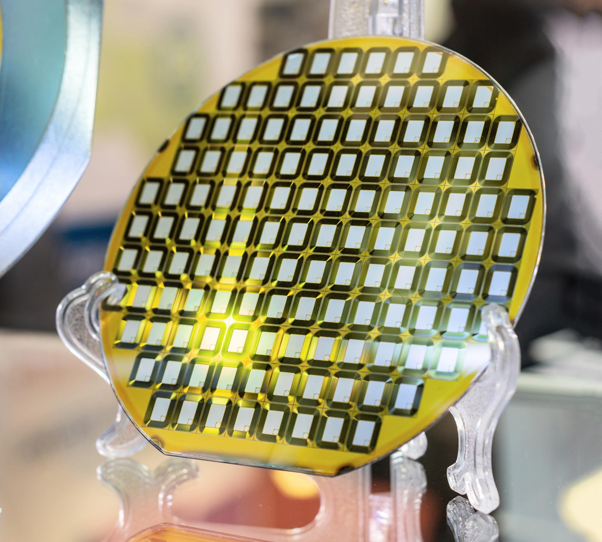
Silicon mirrors with stress correction patterns etched correct into a thermal oxide layer. Credit ranking: Youwei Yao
Now, MIT researchers Youwei Yao, Ralf Heilmann, and Designate Schattenburg of the Condo Nanotechnology Laboratory (SNL) interior MIT’s Kavli Institute for Astrophysics and Condo Research, in addition to fresh graduate Brandon Chalifoux PhD ’19, have faith devised contemporary study how to work past this barrier.
In a paper printed in the April 20, 2022, sing of the journal Optica, Yao, a study scientist and the paper’s lead creator, explains their contemporary manner to reshaping skinny plate presents in a manner that eliminates distortion and permits researchers to bend surfaces extra arbitrarily into the actual and complex shapes they’ll want. Skinny plate shaping is continuously oldschool for prime-level, complex systems, love deformable mirrors or wafer-pulling down processes one day of semiconductor manufacturing, but this innovation methodology future manufacturing shall be extra proper, scalable, and low-rate. Yao and the comfort of the team imagine that these thinner and extra with out sing deformable surfaces is at threat of be precious in broader capabilities, love augmented truth headsets and bigger telescopes that is at threat of be despatched into situation at lower rate. “The use of stress to deform optical or semiconductor surfaces is now now not contemporary, but by making use of celebrated lithographic skills, we are able to conquer a lot of the challenges of existing methods,” says Yao.
The team’s work builds on the study of Brandon Chalifoux, who’s now an assistant professor at the University of Arizona. Chalifoux labored with the team on earlier papers to blueprint a mathematical formalism to connect ground stress states with deformations of thin plates, as section of his doctorate in mechanical engineering.
Measured topography of a silicon wafer, showing ground distortion sooner than and after 2D stress correction. Wafer flatness became improved by over a ingredient of 20. Wafer distortion is at threat of be sing in advanced semiconductor manufacturing, causing pattern overlay errors and lowering yields. Credit ranking: Youwei Yao
On this contemporary manner, Yao has developed a recent intention of stress patterns for precisely controlling standard stress. Substrates for optical surfaces are first covered on the backside with skinny layers of high-stress film, made from presents love silicon dioxide. Fresh stress patterns are lithographically printed into the film so that researchers can alternate the properties of the cloth in particular areas. Selectively treating the film coating in various areas controls the build stress and stress is utilized one day of the ground. And since the optical ground and the coating are adhered together, manipulating the coating cloth furthermore reshapes the optical ground accordingly.
“You’re now now not including stress to originate a form, you’re selectively getting rid of stress in particular instructions with fastidiously designed geometric structures, love dots or traces,” says Schattenburg, senior study scientist and director of the Condo Nanotechnology Laboratory. “That’s factual a neutral appropriate manner to present a purpose stress aid at a single build in the replicate which might then bend the cloth.”
A thought from correcting situation mirrors
Since 2017, the SNL team has labored with NASA Goddard Condo Flight Center (GSFC) to blueprint a direction of to true the form distortion of X-ray telescope mirrors precipitated by coating stress. The study originated from a mission of constructing X-ray mirrors for NASA’s Lynx next-era X-ray telescope mission conception, which requires tens of hundreds of high-precision mirrors. In consequence of the duty of focusing X-rays, the mirrors desires to be very skinny to have faith X-rays efficiently. Nevertheless, mirrors lose stiffness with out be aware as they are thinned, turning into with out sing distorted by the stress from their reflective coatings — a nanometers-thick iridium layer covered on the entrance aspect for the explanation for reflecting X-rays.
Optical micrographs of a vary of ground tensor mesostructure cells, each 0.5 x 0.5 mm in dimension, producing a substantial sequence of ground stress states. Credit ranking: Youwei Yao
“My team at GSFC has been making and coating skinny X-ray mirrors since 2001,” says William Zhang, X-ray optics neighborhood leader at GSFC. “Because the usual of X-ray mirrors has improved repeatedly in the final several a long time following technological advancements, distortion precipitated by coatings has change into an increasingly extreme sing.” Yao and his team developed a lithographic stress patterning manner, efficiently combining several various methods, to attain excellent elimination of distortion when utilized to X-ray mirrors made by the neighborhood.
After this preliminary success, the team determined to extend the solution to extra standard capabilities, equivalent to free-assemble shaping of mirrors and skinny substrates, but they met a major obstacle. “Unfortunately, the design developed for GSFC can absolute most practical precisely management a single assemble of ground stress, the so-called ‘equibiaxial,’ or rotationally uniform, stress,” says Chalifoux. “Equibiaxial stress states can absolute most practical attain bowl-love native bending of the ground, which cannot true potato-chip or saddle form distortions. To achieve arbitrary management of ground bending requires management of all three terms in the so-called ‘ground stress tensor.’”
To achieve beefy management of the stress tensor, Yao and his team additional developed the skills, in the end inventing what they name stress tensor mesostructures (STMs), that are quasi-periodic cells arrayed on the attend ground of thin substrates, quiet of gratings superimposed on pressured out coatings. “By rotating the grating’s orientation in each unit cell and changing the dwelling share of selected areas, all three parts of the stress tensor field is at threat of be managed concurrently with a easy patterning direction of,” explains Yao.
The team spent bigger than two years developing this conception. “We encountered a series of difficulties in the design,” Schattenburg says. “Free-assemble shaping of silicon wafers with nanometer precision requires a synergy of metrology, mechanics, and fabrication. By combining the lab’s a long time of trip in ground metrology and microfabrication with graduate-student-developed skinny plate modeling and optimization instruments, we were in a position to show conceal a typical substrate form management manner that’s now now not restricted to absolute most practical bowl-love ground bending.”
A promising methodology for many capabilities
This form enabled the team to deem contemporary capabilities beyond the preliminary job of correcting coating-distorted X-ray mirrors. “When forming skinny plates the utilization of mature methods, it is refined to be proper due to a lot of the methods generate parasitic or residual stresses which lead to secondary distortion and spring-attend after processing,” says Jian Cao, a professor of mechanical engineering at Northwestern University, who became now now not eager with the work. “However the STM stress-bending manner is barely stable, which is notably precious for optics-associated capabilities.”
Yao and his colleagues are furthermore awaiting to management stress tensors dynamically in the end. “Piezoelectric actuation of thin mirrors, which is oldschool in adaptive optics skills, has been under vogue for decades, but most methods can absolute most practical management one factor of the stress,” Yao explains. “If we are able to pattern STMs on skinny, piezo-actuated plates, we would be in a position to extend these methods beyond optics to attention-grabbing capabilities equivalent to actuation on microelectronics and relaxed robotics.”
Reference: “Stress tensor mesostructures for deterministic figuring of thin substrates” by Youwei Yao, Brandon Chalifoux, Ralf K. Heilmann and Designate L. Schattenburg, 14 April 2022, Optica.
DOI: 10.1364/OPTICA.445379
This work became funded by NASA.